The 555-timer astable circuit is widely used, so I will use it in this development example.
Most of the following work will be done by starting standalone programs from the Kicad project manager.
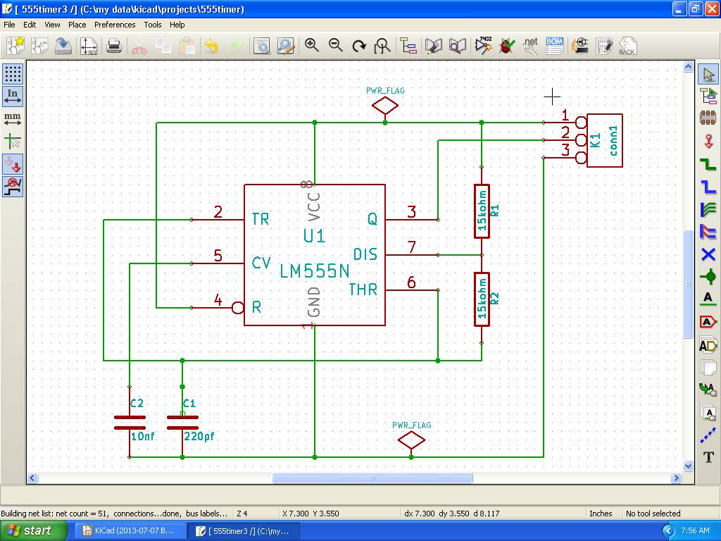
First, a schematic must be created using the EESchema schematic editor.
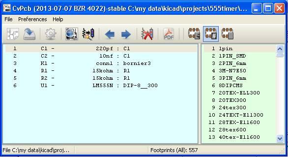
Then each component is assigned a footprint with the CVPcb footprint selector.
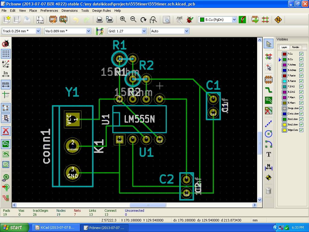
Then it is time to do the PCB layout with the PCBnew editor.
After the layout is done, other new files can be created as needed.
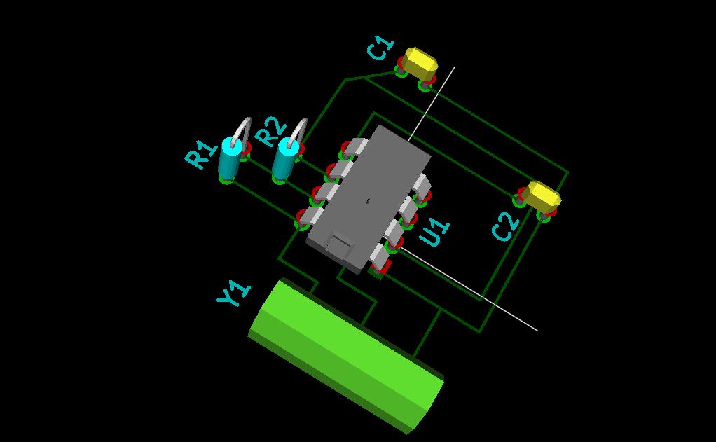
These files include Gerber files, drilling files, and more. Below is a 3-D image file.
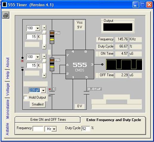
Here a standalone stimulation program is used to see how the circuit should run.
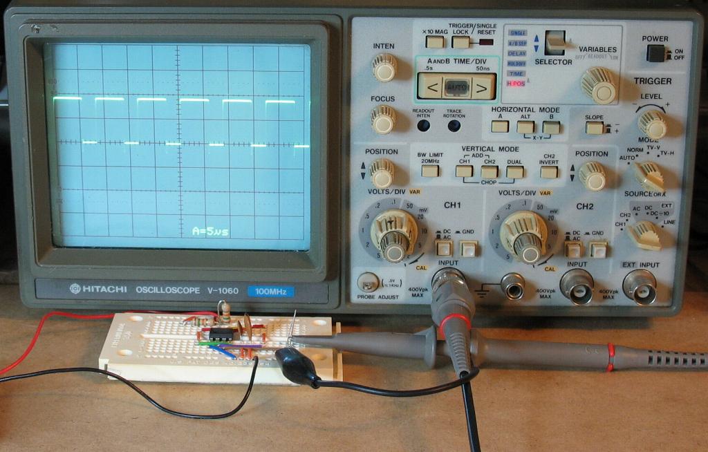
Finally, a breadboarded 555 circuit is tested with a scope to verify proper function.